Sweep the coupler gap
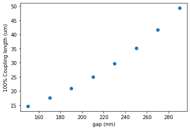
Analytic calculation of 100% coupling length into two parallel SOI waveguides with a varying gap at different TE wavelengths.
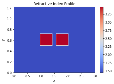
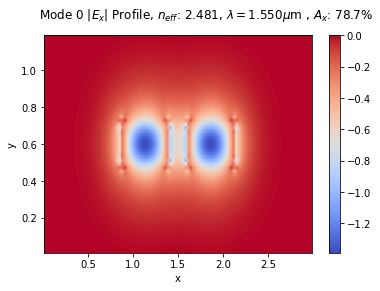
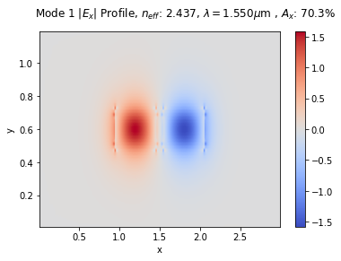
An example refractive index profile for the two waveguides spaced 200nm is shown.
[1]:
import numpy as np
import matplotlib.pyplot as plt
import modes as ms
import opticalmaterialspy as mat
from modes.design import directional_coupler_lc

wavelength_nm  = 1550
width = 0.45
thickness = 0.22
widths = [width]*2
wg_gaps = np.arange(0.15, 0.30, 0.05)
wg_gaps = np.array([0.15, 0.2, 0.25])
dcs = [ms.waveguide_array(widths=widths, wg_gaps=[wg_gap], sub_width=3, thickness=thickness) for wg_gap in wg_gaps]
dcs[0]
[1]:
[0.45, 0.45] x 0.22 um, n_wg = 3.4757, n_clad = [1.444023621703261]

[2]:
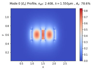
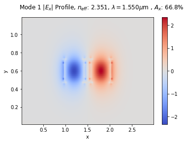
ms.mode_solver_full(wg=dcs[0], n_modes=2, plot=True, plot_index=True, fields_to_write=('Ex'))
[2]:
<modes._mode_solver_full_vectorial.ModeSolverFullyVectorial at 0x7f358d06a3d0>
[3]:
n_effs = [ms.mode_solver_full(wg=wg, n_modes=2).results['n_effs'] for wg in dcs]
[4]:
ne = [ n_eff[0].real for n_eff in n_effs]
no = [ n_eff[1].real for n_eff in n_effs]
[5]:
lc = [directional_coupler_lc(wavelength_nm, n_eff_1, n_eff_2) for n_eff_1, n_eff_2 in zip(ne, no)]
[6]:
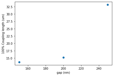
plt.plot(wg_gaps*1e3, lc, 'o')
plt.xlabel('gap (nm)')
plt.ylabel('100% Coupling length (um)')
[6]:
Text(0, 0.5, '100% Coupling length (um)')
[7]:
# to increase reduce the gap step we need to reduce the size of the x_step and y_step computing grid

wg_gaps = np.arange(0.15, 0.30, 0.02)
dcs = [ms.waveguide_array(widths=widths, wg_gaps=[wg_gap], x_step=0.01, y_step=0.01) for wg_gap in wg_gaps]
n_effs = [ms.mode_solver_full(wg=wg, n_modes=2).results['n_effs'] for wg in dcs]
ne = [ n_eff[0].real for n_eff in n_effs]
no = [ n_eff[1].real for n_eff in n_effs]
lc = [directional_coupler_lc(wavelength_nm, n_eff_1, n_eff_2) for n_eff_1, n_eff_2 in zip(ne, no)]
[8]:
plt.plot(wg_gaps*1e3, lc, 'o')
plt.xlabel('gap (nm)')
plt.ylabel('100% Coupling length (um)')
[8]:
Text(0, 0.5, '100% Coupling length (um)')
Exercise
Design a directional coupler with a gap of 250nm that will tap off 10% of the optical power at a wavelength of 1550nm. What length in microns does the directional coupler have to be?
[9]:
directional_coupler_lc?
[10]:
wavelength_nm  = 1550
width = 0.5
thickness = 0.22
widths = [width]*2
dc = ms.waveguide_array(widths=widths, wg_gaps=[0.25], sub_width=3, thickness=thickness)
[11]:
ms.mode_solver_full(wg=dc, n_modes=2, plot=True, plot_index=True, fields_to_write=('Ex'))
[11]:
<modes._mode_solver_full_vectorial.ModeSolverFullyVectorial at 0x7f358c707be0>


[12]:
directional_coupler_lc(1550, 2.481, 2.464, power_ratio=0.1)
[12]:
9.337964273048785
Exercise
What is the coupler length (in µm) that corresponds with 100% power transfer from the through port (top) to the cross port (bottom)? Assume 500nm x 220nm Si waveguides in SiO2, 1550 nm wavelength, and a 100 nm coupler gap
[13]:
dc = ms.waveguide_array(widths=widths, wg_gaps=[0.1], sub_width=3, thickness=thickness, x_step=0.01)
m = ms.mode_solver_full(wg=dc, n_modes=2, plot=True, fields_to_write=('Ex'))

[14]:
directional_coupler_lc(1550, np.abs(m.n_effs)[0], np.abs(m.n_effs)[1], power_ratio=1)
[14]:
12.5925379514069
[15]:
directional_coupler_lc(1550, 2.498, 2.437, power_ratio=1)
[15]:
12.704918032786805
[ ]: